TSMC
 Asian manufacturer ready to begin research for 2 nm nodes
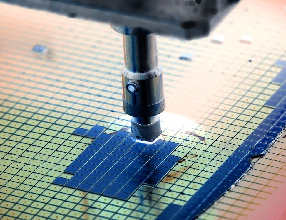
The race for miniaturization continues, the TSMC is first to announce R & D for the 2 nm node, which will be built at the 3 nm facility from Hsinchu, Taiwan. TSMC plans to complete the 3 nm facility by 2021 and begin 3 nm mass production in 2022, so the 2 nm node is expected to become operational around 2024.
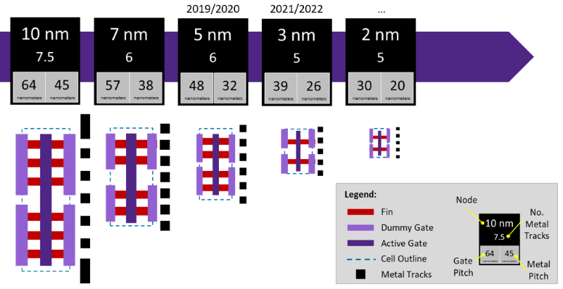
Samsung and TSMC are the only foundries expected to have fully operational 5 nm production by 2020, but both companies already announced plans for 3 nm nodes. Even though the performance gains are not significant beyond 7 nm, every new miniaturization achievement will ensure important production contracts coming from fab-less companies like AMD, Qualcomm and Nvidia.
Just recently, Samsung managed to scoop important deals involving Nvidia's upcoming Ampere GPUs and Qualcomm's next gene Snapdragon 865 SoC right from under TSMC's nose, as the Taiwanese foundries are currently overbooked on the 7 nm nodes, plus Samsung appears to have better 7 nm EUV nodes . To counter this move, TSMC immediately stepped forward announcing that it is ready to begin R & D for a 2 nm node.
 Chinese publication TechWeb reports that TSMC spokesperson Zhuang Zishou essentially confirmed that the 2 nm node will be built in the 3 nm facility from Hsinchu, Taiwan. TSMC is looking to begin construction of the 3 nm facility some time in 2020, complete it by the end of 2021 and begin 3 nm mass production in 2022. The 2 nm is expected to become operational in 2024.
It will be interesting to see how TSMC is going to handle miniaturization beyond 1 nm. There are already a few alternatives to silicon, but it will most likely come down to the easiest and cheapest way to implement the modified processes. by Bogdan Solca


No comments:
Post a Comment