TECH
Russia recently unveiled a lithography tool with 350nm technology that is decades behind its competitors
Russia recently completed the development of its first domestic lithography tool aimed at chip manufacturing processes in the 350 nanometer (nm) range.
The equipment was created in partnership between the Zelenograd Nanotechnology Center (ZNTC) and the Belarusian company Planar, and has already passed official inspections and is currently in the integration phase in Zelenograd.
Despite the symbolic milestone and the technological independence it represents, the project raises doubts as to its commercial viability, since its design dates back to industrial standards from the 1990s.
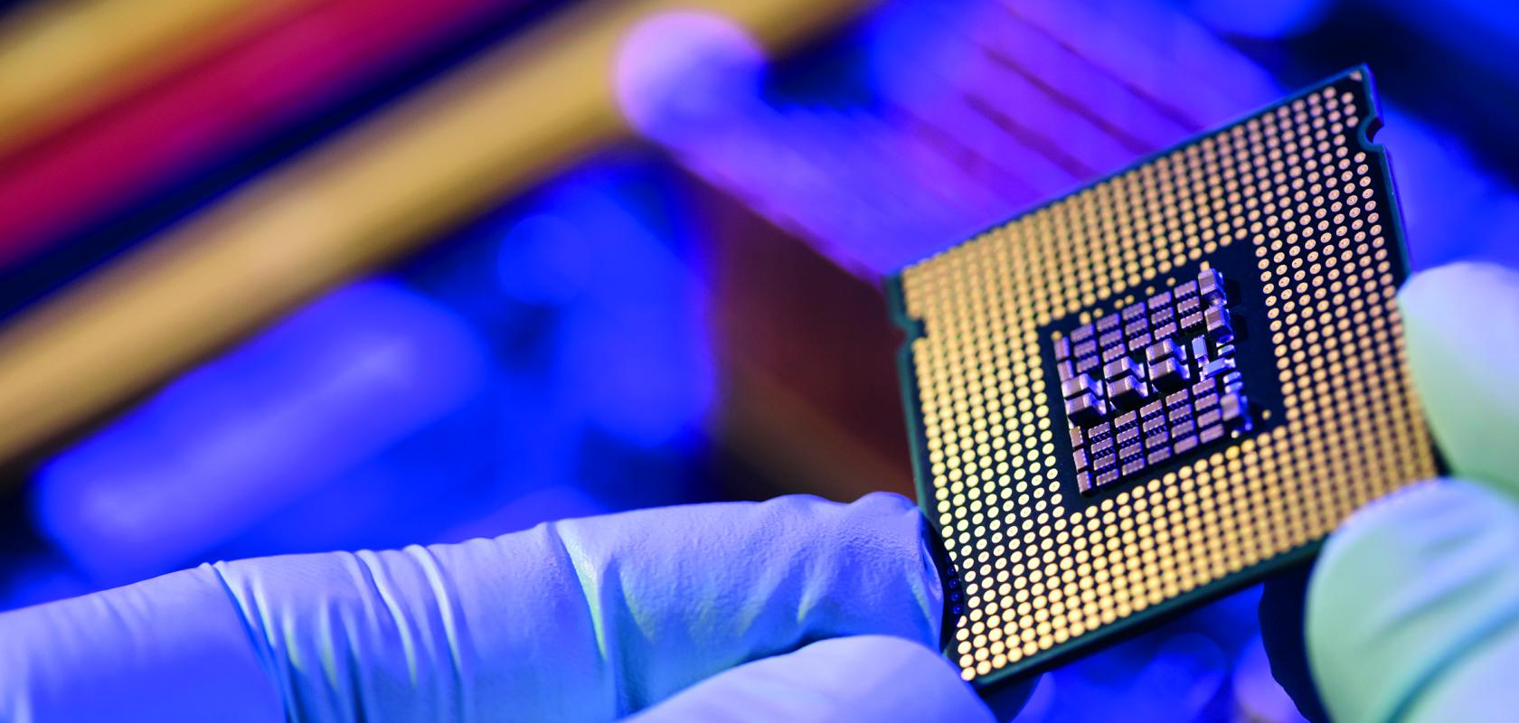
A basis for future developments, but limited at present...ZNTC's new system is compatible with 200 mm wafers and uses a solid-state laser as the light source for chip exposure. The exposure field is 22 mm x 22 mm, equivalent to 484 mm². However, key technical details such as the laser’s power and wavelength have not yet been disclosed.
The use of a solid-state laser is unusual among leading lithography equipment manufacturers such as ASML, which have for decades used mercury lamps (i-line at 365 nm) and excimer lasers such as KrF (248 nm) and ArF (193 nm) for processes between 350 nm and 130 nm. ZNTC has not disclosed whether its light source follows this standard or is an alternative solution, which raises speculation about its future plans.
Although the 350nm process is obsolete by modern standards, it still finds applications in sectors such as automotive, energy management and military equipment, where extreme miniaturization is not a requirement.
In addition, the new equipment could be used in non-critical production layers, or even in activities such as defect analysis, wafer marking and micromachining – roles for which solid-state lasers are more common.
Out of step with the global (and even national) pace...Even Russia's own leading chip manufacturers, such as Mikron and Angstrem, already operate with more advanced production nodes, ranging from 250nm to 90nm, which further limits the immediate applicability of the new machine.
These manufacturers, in fact, continue to depend on ASML equipment, mainly models from the PAS 5500 series, often imported in parallel to circumvent sanctions.
The project is part of an ambitious plan by the Russian government...Despite the delay, the machine developed by ZNTC can be seen as a first step within a strategic plan by the Russian government to achieve autonomy in semiconductor manufacturing in the future. The national roadmap foresees the arrival of the 90nm process by the end of 2025, with goals of reaching 28nm in 2027 and 14nm in 2030.
ZNTC itself is already working on a more advanced model, which aims to process 130nm lithography and is scheduled for completion in 2026.
The expectation is that this version will incorporate learnings from the current machine and bring specifications more aligned with the needs of the national industry.
The first step on a still long path...Russia's new lithography tool is indeed an important advance in terms of technological sovereignty, but its practical usefulness is limited in the short term due to technological backwardness.
However, it can serve as a basis for the development of more modern tools, as the country seeks to become less dependent on Western technologies and circumvent international sanctions.
While Russia is making up for technological losses with ambitious plans until 2030.
mundophone


No comments:
Post a Comment