TECH
Panther Lake teardown reveals Intel 18A in detail — TSMC still leads in density
SemiAnalysis has taken Intel’s Panther Lake apart, showing how the company’s 18A process combines RibbonFET gate-all-around transistors with PowerVia backside power delivery. The analysis finds that 18A delivers logic density similar to TSMC’s N3E, but does not yet give Intel a clear manufacturing lead over TSMC’s newer nodes.
SemiAnalysis has taken a deep look inside Intel’s Core Ultra 7 365 (Panther Lake) processor, offering a first independent look at what is inside the chips and at Intel’s most advanced chipmaking technology to date. The analysis focuses on Intel’s 18A process, including its new transistor design and backside power-delivery system — two technologies the company sees as central to its manufacturing comeback.
Intel’s Panther Lake is more than a new laptop processor. It is the first consumer product to put Intel’s 18A manufacturing process into customers’ hands. In a teardown of a Core Ultra 7 365, SemiAnalysis examined the package, its individual silicon tiles, and cross-sections reaching down to the transistors. The result offers a close look at how Intel’s manufacturing plans work in a shipping chip.
The central change is RibbonFET, Intel’s version of a gate-all-around transistor. Its gate surrounds four stacked silicon channels, giving engineers tighter control over current. Panther Lake also introduces PowerVia, which delivers power through wiring behind the transistors. Moving much of that wiring off the front leaves more room for signal connections. Both changes add manufacturing complexity, and SemiAnalysis notes tradeoffs in capacitance and heat flow.
The package shows why calling Panther Lake an “18A chip” needs some care. Its compute tile uses Intel 18A, but the graphics tile varies by model: the smaller version uses Intel 3, while the larger, 12-core version uses TSMC N3E. The I/O tile uses TSMC N6. Intel joins the tiles on a passive silicon base with Foveros-S packaging. That arrangement lets it reserve its newest process for the CPU while choosing other processes for graphics and external connections.
SemiAnalysis measured similar logic density in Panther Lake’s 18A compute tile and its N3E graphics tile. It did not find a peak-density lead over newer competing processes. That distinction captures the teardown’s main finding: Panther Lake proves Intel can ship gate-all-around transistors and backside power together at consumer scale, but the silicon alone cannot establish a lasting manufacturing lead. Performance, production cost, yield, and Intel’s next products will determine how far 18A takes it.
The key finding is that Intel has successfully put both technologies into a real consumer chip. But the teardown also suggests that 18A is roughly on par with TSMC’s N3E in logic density. The names “18A” and “N3E” should not be read as literal physical dimensions 1,8 and 3nm respectively, however: they are node labels rather than directly comparable measurements.
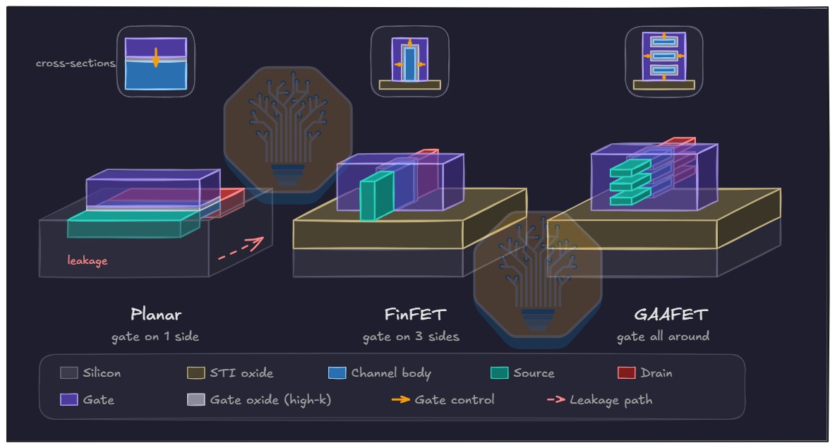
Panther Lake is Intel’s first consumer processor to use RibbonFET transistors, the company’s version of gate-all-around (GAA) technology. Rather than sending current through the narrow vertical “fins” used in older FinFET designs, RibbonFET uses four stacked horizontal silicon sheets. The transistor gate surrounds each sheet, giving Intel tighter control over the electrical current flowing through the transistor and helping to reduce leakage.
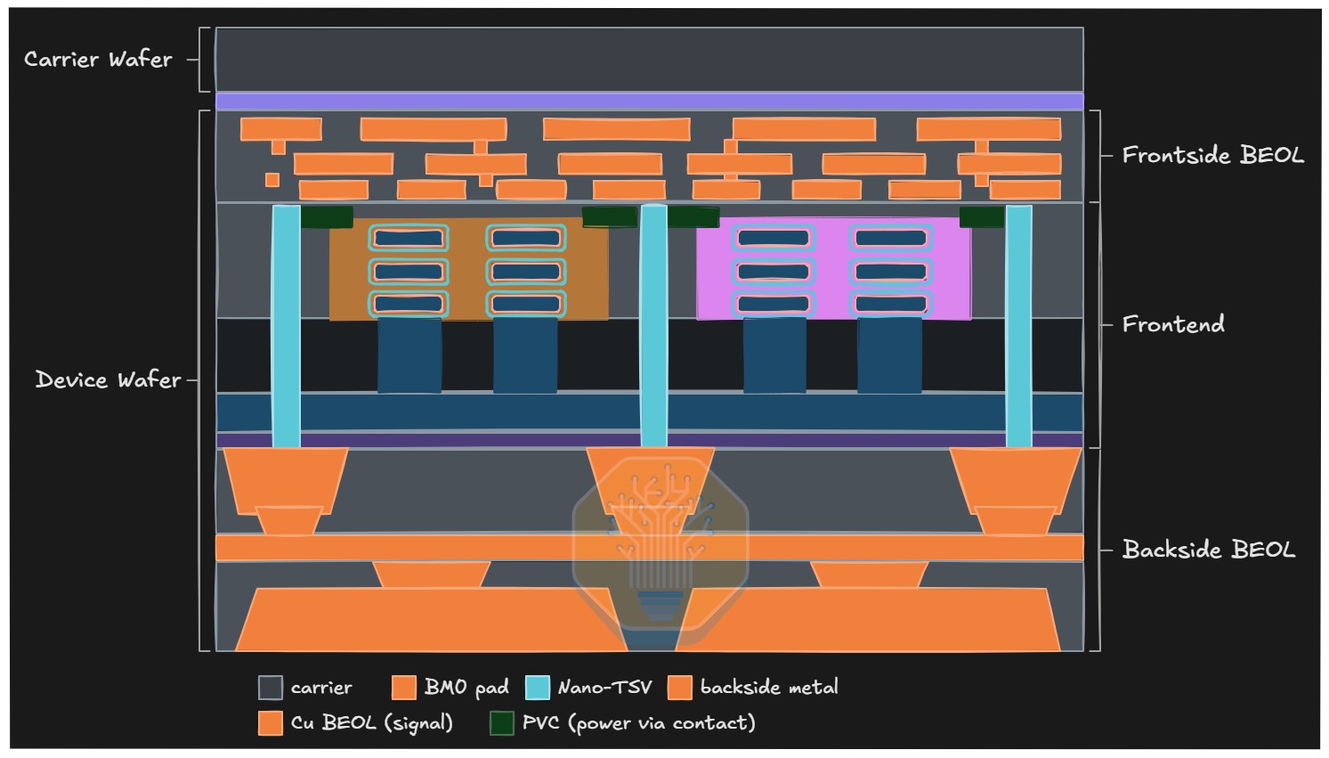
The other major change is PowerVia, Intel’s implementation of a backside power-delivery system. In a conventional processor, power and data signals travel through the metal wiring layers above the transistors. PowerVia moves much of the power network to the other side of the chip, underneath the transistor layer. That frees frontside wiring for signals and enables shorter, wider power paths, potentially reducing electrical resistance and improving voltage stability for the chip’s most demanding blocks.
One of the most interesting findings from the teardown concerns transistor density, which gives us a more restrained view of 18A’s competitive position. SemiAnalysis measured Panther Lake’s 18A compute logic and found that it has roughly the same density as the GPU logic manufactured on TSMC’s N3E process. This is a significant result for Intel, which in recent years has lagged behind the largest contract chip manufacturers in advanced manufacturing processes. However, SemiAnalysis says 18A does not lead TSMC’s newer N3P and N2 nodes, or Samsung’s SF2, in peak density.
That matters because transistor density remains one of the clearest indicators of a manufacturing node’s potential cost and scaling advantages. Intel’s approach may still produce benefits in power delivery, routing flexibility and performance, but it does not automatically translate into the smallest possible logic area.
The analysis also shows how Intel is using chiplets and advanced packaging to combine different process technologies in one product. The processor combines separate compute, GPU and I/O tiles on a passive silicon base using Foveros-S packaging. The compute tile is made on Intel 18A, while the GPU comes in two versions: a four-core Xe3 tile produced on Intel 3, and a larger 12-core version manufactured by TSMC using N3E. The I/O tiles are also made by TSMC, using its older N6 process.
SemiAnalysis found notable changes inside the compute tile as well. The teardown indicates that Panther Lake’s CPU architecture is an evolution rather than a complete redesign. Its Cougar Cove performance core remains close in area to the Lion Cove core used in the previous-generation Lunar Lake, even as L2 cache capacity rises from 2.5 MB to 3 MB per core. SemiAnalysis estimates that Cougar Cove fits 20 % more L2 cache into a similarly sized core area. Meanwhile, the four-core Darkmont LP E-core cluster is about 5 % smaller than its predecessor.
The teardown also points to an efficiency-focused redesign of Intel’s AI accelerator. Panther Lake’s NPU 5 is said to take up 36.9 % less area than the NPU 4 in Lunar Lake while keeping the same overall INT8 MAC count. Intel consolidated processing into fewer, larger neural compute engines and reduced the number of scratchpad memories and SHAVE DSPs from 12 to six. NPU 5 also adds native FP8 support, a lower-precision data format increasingly used for AI inference.
The GPU offers another interesting comparison. An Xe3 core in the Intel 3-based GT1 tile is about 55 % larger than one in the 12-core N3E-based GT2 tile. Put simply, Intel’s own process can produce the GPU, but TSMC’s N3E allows Intel to fit substantially more graphics hardware into the same silicon area.
mundophone




No comments:
Post a Comment