TECH
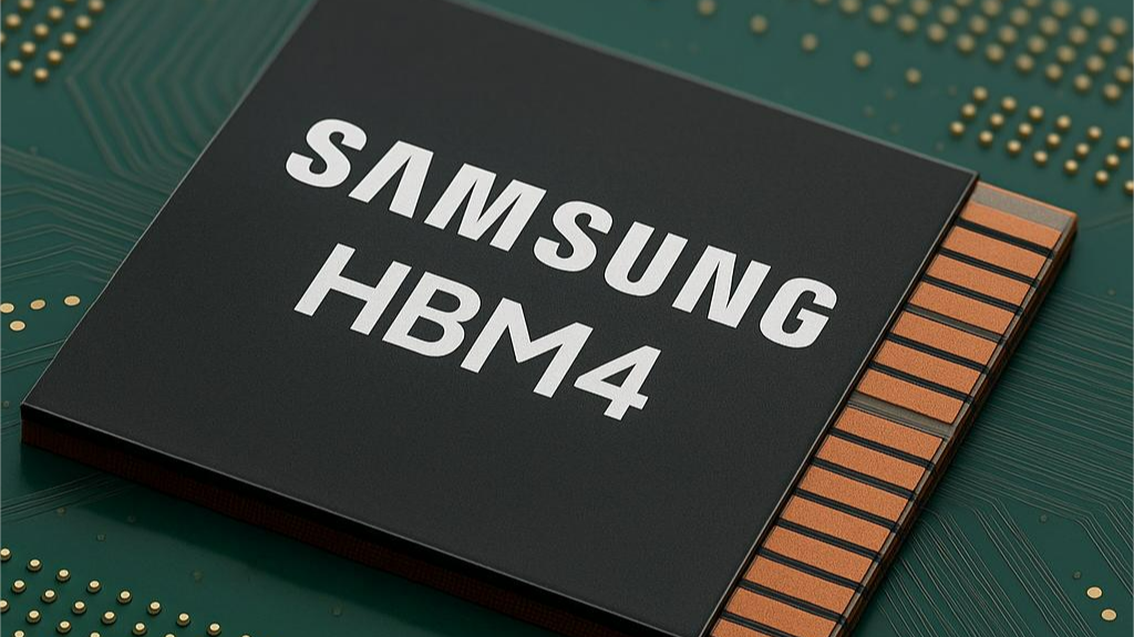
Samsung takes the lead in AI with mass production of HBM4 chips
Samsung Electronics has just marked a historic turning point in the semiconductor industry. In an announcement that is shaking up global technology markets, the South Korean giant confirmed that it is the first company in the world to begin mass production of the sixth generation of high-bandwidth memory, known as HBM4. This advancement is not just a technical upgrade; it represents the brand's triumphant return to the top of a sector where it had recently lost ground to rivals such as SK hynix and Micron.
If you follow the hardware market, you know that artificial intelligence (AI) demands unprecedented data processing speed. HBM4 chips were specifically designed to power the best AI accelerators on the planet, ensuring that the flow of information between the processor and memory does not become an obstacle. As a technology enthusiast, you realize that this step puts Samsung in a privileged position to dominate the supply of critical components for companies developing complex language models and cloud computing infrastructure.
This announcement comes at a crucial time. After a 2025 marked by some production challenges and competitive pressure, Samsung decided to go all-in on radical innovation. The company didn't just follow industry standards; it decided to raise the bar and set new performance metrics that, until now, seemed unattainable for direct competitors in the short term.
To achieve these impressive results, Samsung turned to its most advanced 1c DRAM technology, which uses a sixth-generation 10-nanometer class. This is currently the most sophisticated manufacturing technique on the market. By combining this with a 4-nanometer manufacturing process from its foundry division, you get a chip that is not only extremely fast but also much more energy-efficient.
The issue of efficiency is vital if you think about the colossal power consumption of modern data centers. Samsung managed to ensure stable production yields, meaning it can manufacture these units in large quantities without compromising quality or reliability. This stability is what allows the brand to start shipping the first consignments to customers immediately, gaining a precious time advantage over its competitors.
The integration between Samsung's memory division and its foundry division was key to success. By controlling the entire production ecosystem, engineers were able to optimize the design of the HBM4 chips in a way that companies relying on third parties for manufacturing have difficulty replicating. This is the kind of vertical integration that allows the South Korean brand to dictate the pace of the semiconductor market.
Speeds that surpass all industry standards... When we look at the pure numbers, the performance of these new chips is astonishing, to say the least. Samsung's HBM4 memory operates at a speed of 11.7 Gbps. If you compare that to the JEDEC industry standard, which sets it at 8 Gbps, you'll see a performance increase of about 46%. It's a generational leap that ensures the total bandwidth of a single memory stack can reach 3.3 TB/s, exceeding even the most stringent demands of hardware manufacturers.
Even when compared to the brand's own previous generation, HBM3E, the new HBM4 manages to be 22% faster. You can find these memories in capacities ranging from 24GB to 36GB, but the company has already confirmed that it won't stop there. To meet the memory hunger of the most demanding AI applications, Samsung plans to produce 16-layer versions with capacities reaching 48GB, something that until recently seemed like science fiction.
Samsung's vice president of memory development, Hwang Sang-joon, highlighted that the company decided to break with the tradition of using only already tested processes. By taking risks with cutting-edge technologies like 1c and 4nm DRAM right from the start, they managed to create room for maneuver for future expansion. This means that the HBM4 platform still has room to grow and evolve in the coming months, adapting to the volatile needs of customers.
The roadmap to total dominance by 2027...Samsung's strategy for the coming years is already mapped out and seems unstoppable. In addition to the mass production of HBM4 that is now beginning, the technology company has already confirmed that the HBM4E variant will arrive in the second half of 2026. This will be an even more optimized version, focused on specific niches that require the maximum possible bandwidth. You will probably see these chips in the most powerful supercomputers of the next decade.
But the brand's vision goes further. By 2027, the goal is to introduce customized HBM chips. This will allow specific clients, such as large technology companies that design their own processors, to have memories tailored to their architectures. It's a level of customization that could change how AI devices are built, integrating memory even more deeply into the heart of the system.
While the current focus is on mass production, Samsung is already working behind the scenes on the successor HBM5. This cycle of continuous innovation serves to ensure that the now-regained leadership is not lost again. For you, who follow these developments, it's clear that the battle for semiconductors has entered a phase of maximum acceleration, and Samsung has just stepped on the accelerator with a force that its rivals will have difficulty matching.
mundophone


No comments:
Post a Comment