TECH
ASML's triple-laser EUV tech breakthrough aims to boost chip production by 50%
You know who ASML is, right? For those who are just joining us, ASML is the guys who make the tools that the TSMC and Intel and Samsung guys use to make their bleeding-edge chips. The Dutch company is the only firm in the world capable of commercializing Extreme Ultra-Violet (EUV) lithography machines, which are absolutely vital to the production of chips with ludicrously small feature sizes. The company says it has created a new system that utilizes three separate laser bursts to apply up to 1000W of EUV power to the photoresist on a wafer, which in turn could allow it to increase wafer production by 50%.
So, lithography is etching things into stone; in this case, the stone is silicon. The way photolithography works is that you lay down a material called photoresist in dense patterns, and then you blast it with photons to "dose" the photoresist and induce a chemical structure change. It's just like photography; too much light and it's overexposed, too little and it's underexposed. Both are bad.
The 'dosing' requirement is fixed according to the process, so each square centimeter of a wafer must receive a certain number of photons. Increasing the source power, in this case all the way to 1 kilowatt, allows you to reach the correct amount of energy applied to the photoresist more quickly. This, in turn allows you to turn out chips faster: up to 330 wafers per hour, which is directly 50% more than the current fastest rate of 220 wafers per hour.
Machines could process 330 wafers an hour by 2030...Van Gogh said customers should be able to process about 330 silicon wafers an hour on each machine by the end of the decade, up from 220 now. Depending on the size of a chip, each wafer can hold anywhere from scores to thousands of the devices.
ASML got the power boost by doubling down on an approach that already places its machines among the most complex inventions of humans.
To produce light with a wavelength of 13.5 nanometers, ASML's machine shoots a stream of molten droplets of tin through a chamber, where a massive carbon dioxide laser heats them into plasma.
This is a superheated state of matter in which the tin droplets become hotter than the sun and emit EUV light, to be collected by precision optic equipment supplied by Germany's Carl Zeiss AG and fed into the machine to print chips.
The key advancements in Monday's disclosure involved doubling the number of tin drops to about 100,000 every second, and shaping them into plasma using two smaller laser bursts, as opposed to today's machines that use a single shaping burst.
"It's very challenging, because you need to master many things, many technologies," said Jorge J. Rocca, a professor at Colorado State University whose lab focuses on laser technologies and has trained several ASML scientists.
"What was achieved - one kilowatt - is pretty amazing."
ASML believes the techniques it used to hit 1,000 watts will unlock continued advances in the future, Purvis said, adding, "We see a reasonably clear path toward 1,500 watts, and no fundamental reason why we couldn't get to 2,000 watts."
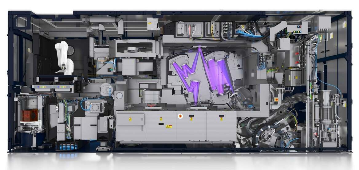
An ASML TwinScan EUV machine. above: a render of the inside(image above)
So what's up with the three lasers? Well, current methods already use one laser pulse to shape the droplets of molten tin and then a second to turn them into plasma. That plasma is where the EUV radiation comes from, by the way. The key advancement in the new machines seems to be using one laser to to flatten the droplets before using a second laser to "rarefy" them, or turn them into a fine mist. After that, the main laser pulse turns them into plasma, emitting the necessary EUV light.
If that sounds like an unbelievably convoluted process, you're not wrong, but that's exactly the lengths we've had to stride to approach the ability to make microprocessors that fit hundreds of billions of discrete components into a rock the size of a postage stamp. Remember vacuum tubes? Each one of those was functionally equivalent to one of the billions of parts in a modern microchip. It is not an exaggeration to say that microprocessors are the ultimate achievement of human civilization.
To bring things back to earth, though, this development is still in the research phase, not in the productization phase. We're not going to see a new TwinScan machine that sports the enhanced tri-laser tech later this year. ASML told Tom's Hardware that this system, along with a new tin droplet technique, will "take years before [they are] commercialized." In fact, this tech isn't even on the roadmaps yet this year, so it'll be a while before Intel, TSMC, or anyone else see the benefits of this breakthrough. Still, it shows that ASML isn't resting on its laurels, and that its new competitors in the US and elsewhere have a lot of ground to cover to catch up.
mundophone


No comments:
Post a Comment