TECH
China unveils first breakthrough in domestic silicon photonics chip technology
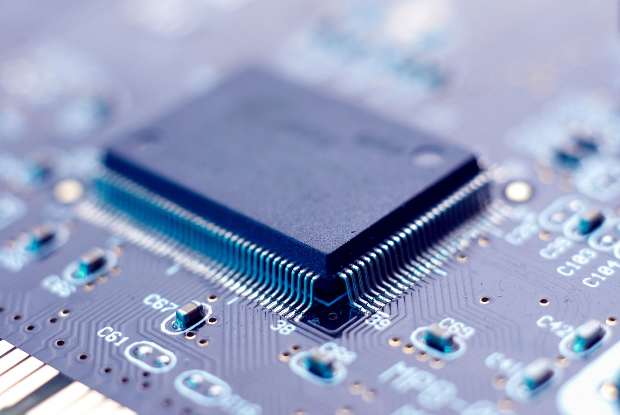
China's state-backed JFS Laboratory has unveiled the country's first silicon photonics chip, a significant advancement that could revolutionize AI and high-performance computing. This novel technology uses lasers instead of traditional copper wires, offering increased bandwidth, reduced latency, and improved energy efficiency.
JFS Laboratory, a government-supported company, has just rolled out the country's very first silicon photonics chip. This is a pretty exciting step forward for things like AI and high-performance computing, which need that extra boost.
Silicon photonics uses lasers for input and output instead of the usual copper wires, which has some incredible perks. We're talking about way more bandwidth, less waiting around (latency), and better energy savings—all significant for ramping up AI and HPC systems to match the growing demands.
Processors with laser-based I/O are expected to have particular advantages over traditional chips with copper interfaces in high-performance applications like AI and HPC.
Neither JFS nor SCMP disclose what exactly was achieved and how the silicon photonics chip connects to the processor, so we can only wonder about its characteristics in terms of data transfer rates and power. In fact, the only thing that we know about JFS Laboratory is that it is based in Wuhan and was established in 2021 with 8.2 billion yuan ($1.2 billion) in funding from the government. Therefore, it has taken the company three years to successfully integrate a laser light source into a silicon-based chip.
Silicon photonics is crucial for AI and HPC processors, and infrastructure, because it addresses key limitations of traditional copper-based interconnections. Particular benefits of a successful implementation will be seen in terms of bandwidth, latency, and energy efficiency, just like typical optical interconnects.
Given the context of China amid sanctions and the inability to produce high-performance processors for AI and HPC akin to Nvidia's H100 or AMD's Instinct MI300-series, scalability is perhaps the most important feature enabled by optical interconnects.
The ability to scale up and out computing power without increasing power consumption caused by copper-based interconnects is key for hyperscale AI and HPC datacenters, particularly in Chinese realms. Silicon photonics provides a path for scalable chip designs that can meet the growing computational demands while maintaining efficiency, making it an essential technology for future advancements in artificial intelligence and supercomputing.
Latency is a major factor in scalability. In AI realms, minimizing latency is critical for real-time processing and decision-making. The high-speed, low-latency nature of optical data transfer in silicon photonics allows for faster communication between different parts of the computing system, improving overall performance in applications like AI inference and large-scale simulations. In commercial space, AI-based recommendations software and hardware can also benefit from low latency.
Speaking of commercial AI and HPC applications, we surely should mention power consumption. One of the biggest challenges in AI and HPC is managing the power consumption of datacenters. Silicon photonics is more energy-efficient than copper interconnects, as optical signals generate less heat and require less power to transmit over long distances. As a result, optical interconnects greatly reduce the total cost of ownership (TCO) for datacenters.
In general, JSR seems to have made a breakthrough. However, without actual performance numbers, we can only wonder how significant this breakthrough is.
mundophone


No comments:
Post a Comment