SONY
Company continues to improve its CMOS image sensor
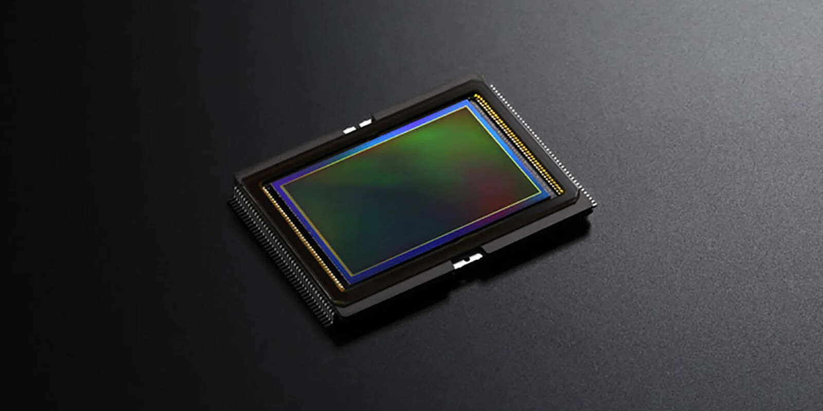
By dispersing the components into additional layers, a better quality image can be extracted from the sensor with a given surface than before.
For years, Sony has been producing image sensors where components are placed on separate layers, which allows for better image quality without the need to increase the size of the sensor. This is especially important for smartphone cameras, as manufacturers don't have the opportunity to put very large sensors there, but of course, these innovations can also be useful in traditional cameras.

The Japanese have now taken another step forward, namely Sony announced the development of its newest sensor, whose great innovation is the separation of the photodiodes that carry out the detection of light and the transistors responsible for its control. In today's sensors, the aforementioned components are placed next to each other within a layer, but in the new development, most semiconductors are banished one level below, to a new layer. This is a logical decision not only because it leaves more room for the photodiodes, thanks to which the sensor's saturation signal level can be doubled (this practically means that the sensor can more accurately interpret the information extracted from the light received in low light conditions, i.e. the dynamic range increases), but in this way the control transistors can also be spread over a larger area. That way, the manufacturer can also use larger transistors to amplify the signals, which will have a good effect on the noise level of the images.
It remains unclear whether Sony will first demonstrate the new sensor on smartphones or on its own Alpha-series cameras, but there's a good chance that the technology will sooner or later be respected in both categories.
Sony

No comments:
Post a Comment