SAMSUNG
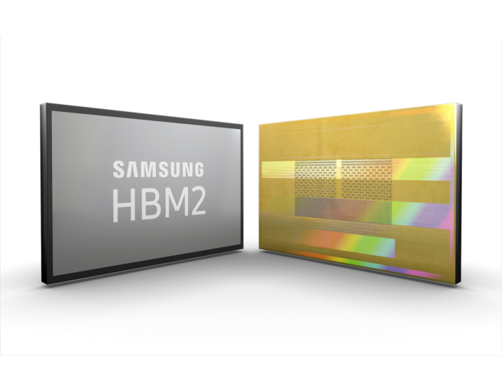
Company completes development of 12-layer 3D TSV DRAM for high-capacity HBM2 modules
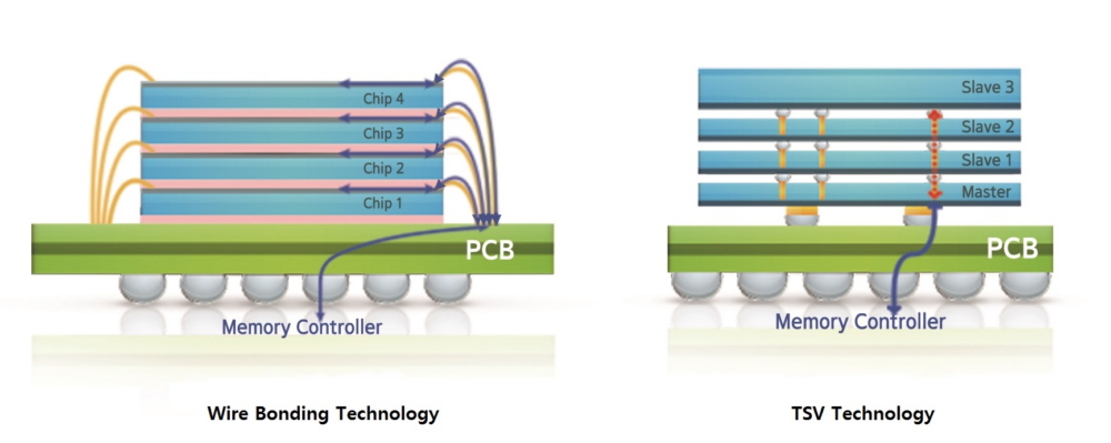
GDDR VRAM seems to be the memory of choice for gaming graphics cards, but GPUs are not exclusively restricted to graphics acceleration anymore. AI and HPC applications together with specialized FPGAs can also benefit from scalable GPU power, but in order to take full advantage of such applications, system integrators need to opt for the more versatile HBM RAM, which can provide higher memory capacity per card via improved packaging. technologies. HBM2 is admittedly slower than the standard GDDR6, yet Samsung's latest breakthrough in DRAM 3D packaging could give the HBM standard the edge it needs.
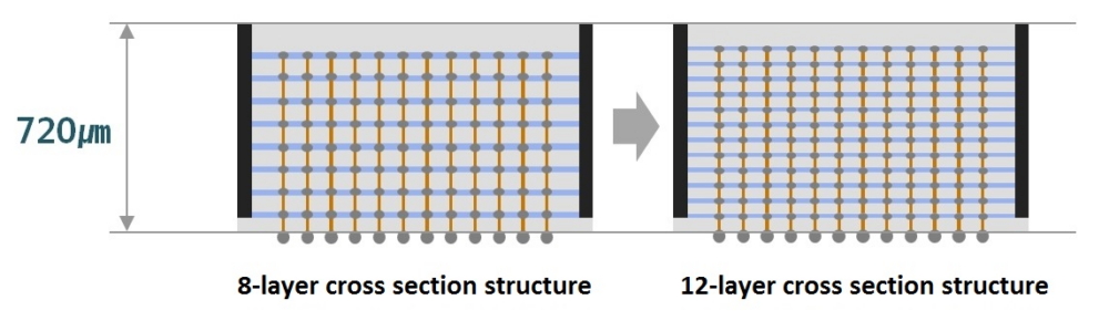
With the jump from 8-layer to 12-layer 3D DRAM packaging, Samsung is opening up ways to overcome the limitations of Moore's law scaling. The 12-layer stack dies feature 60,000 through silicon via holes in the same 720 micron thickness. This allows for thinner DRAM layers, and Samsung admits it needs to tighten the yields as the mass production of such packages is becoming more challenging.
Samsung will first integrate the 12-layer DRAM packaging process in its upcoming 24 GB HBM2 stack dyes. The increased DRAM capacities will allow integrators to add as much as 48 or even 96 GB of memory per card with 2,048 or 4,096-bit buses and significantly increased memory bandwidths. However, 6 and 12 GB configurations are still possible.
No word on pricing for the time being, but, since Samsung is the only one producing the high-capacity HBM2 modules, price points will most likely be higher than those of GDDR6 modules.
by Bogdan Solca


No comments:
Post a Comment